Silicon wafers are key components in semiconductor fabrication process because they act as substrates for most modern semiconductor devices.
What is Semiconductor?
The semiconductor is an element between conductor and insulator, to control movement of carrier(electrons and electron-hole) to generate electric current. Transistor, for example, is the most common to see, which can change the voltage and control magnitude of electric current.
If you comprehend it in a simple way, a transistor is actually like a faucet. When you turn on the faucet, water will flow down.
In the digital world, 0 and 1 are everything, such as text, photos, videos, etc. Therefore, the “off and on” of the transistor faucet corresponds to the “0 and 1” in the digital world. Through the transistor, we can successfully build a bridge between the digital world and the real world.

What is the importance of semiconductor in our daily life?
In fact, semiconductors are used in everyday products like computers, televisions, smartphones, telecommunication, white goods, transportation, banking and even medical diagnostic equipment, and they wouldn’t work without them.

The core of ever-changing tech is the silicon wafer. Chip, or integrated circuit, in computers is from a silicon wafer, and a wafer is from boule.
A die (chip) is a single electrical circuit unit that is positioned on a semiconductor wafer. A grid-like pattern is generated by stacking a large number of dies containing the same electronic circuit on a wafer. A die is similar to a stamp seen on a stamp sheet. They’re eventually diced into individual semiconductor chips, which are subsequently packed to make the final semiconductor product.

Computers were large machines with tubes and dials before silicon-based processors became ubiquitous. They were large, but they were also fragile and less liability because of the quantity of electricity they required.
Tubes were replaced with semiconductor chips, which allowed machines to run faster, cheaper, and more efficiently. Design and size advancements have resulted in light and elegant modern phones and smart equipment in a variety of industries.
According to techopedia, a wafer is a piece of silicon (one of the most abundant semiconductors available worldwide) or other semiconductor material, designed in the form of a very thin disc. Wafers are used to create electronic integrated circuits (ICs) and silicon-based photovoltaic cells. In these designs, the wafer serves as the substrate. Engineers use processes such as doping, implantation and etching to complete the build of the integrated circuit.
These chips seem to be powerful enough to solve the big and small things in our lives and bring convenience, but in fact, they are very fragile and easily damaged. In order for the wafer to be useful, it must have little to no defect.

Why do silicon wafers break easily?
The fact that silicon wafers are easily broken is a material property. It’s for this reason that silicon wafers are so pricey. They’re brittle and simple to break, but they’re not going to fall apart in your hands. They should never be handled with your bare hands since the salt in your sweat will diffuse into the wafer and render it useless.
Wafers can be recycled if they break. In reality, 85% of them are sent back to the manufacturer to be melted down and used to create new wafers.
However, huge loss caused by a broken silicon wafer is beyond your imagination. This necessitates a reverse logistics program, which exacts expenses for actual delivery and causes delays for chip manufacturers and their customers, especially during shortages.

How are silicon wafers shipped?
The fragility of the freight is the first issue to solve in the shipment of semiconductors. This is typically very costly equipment that may be rendered useless in a matter of seconds if it is not manufactured, packaged, and delivered in a clean environment devoid of any dust or debris that could damage the semiconductor’s efficiency.
In reality, semiconductors are produced in cleanrooms for this pristine atmosphere, and electronic components leave the room in special plastic boxes to avoid being damaged or filthy before being tested and packaged.
Several types of commercially available wafer shipment boxes were recommended by fabs as follows, as well as positive test results supported by TSAPPS. These trays or other packaging materials are made out of specialized polymers.
1. Multi-Wafer Horizontal Shipping Boxes
2. Horizontal Stackable Shipping Box
3. Vertical Multiple Wafer Shipping Box
Others, such as waffle packs, blue tape or components delivery formats are common to see.

How to mitigate silicon wafer damage when shipped?
There is no one-size-fits-all solution for preventing product damage. Instead, use a comprehensive strategy that incorporates conventional staff training, shipping best practices, and new technology advancements to prevent the damage that leads to unsaleable items.
One cargo surveyor claims that by taking a thorough approach to transportation and damage mitigation, damage in about 50% of items may be reduced.
Data collection, tracking, and analysis
Companies must gather and evaluate relevant supply chain data to track the success of any policy changes. Data monitors give detailed information about the supply chain, including impact events. Companies can’t react quickly enough to the continually changing dynamics of the supply chain if they don’t have this data. For every type of shipping and every budget, a variety of environmental indicators and recorders are available.

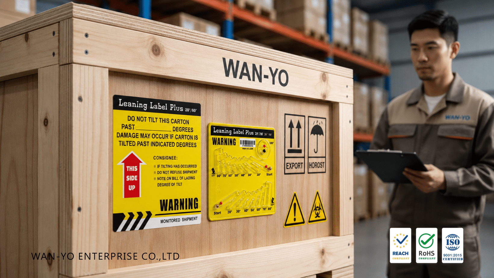
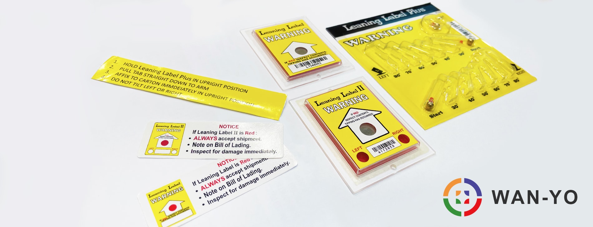
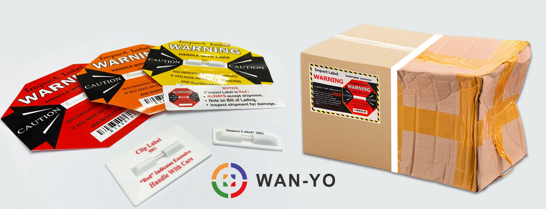
Indicator Labels
For impacts and temperature excursions, simple indicators can provide go/no-go assurance. At predefined impact levels, impact indicators activate and offer a record of potentially harmful falls or drops. Temperature indicators, on the other hand, are activated when temperatures get too hot or too cold.
Indicators placed on the outside of packaging can serve as a visible deterrent to carriers and personnel mishandling packages. Indicators can stimulate product inspections, exposing concealed damage and preventing damaged items from reaching the shelves, because they provide unequivocal evidence of an undesirable event.

Monitors
Data monitors offer a full assessment of supply chain circumstances by capturing the direction, magnitude, and duration of an impact, allowing management to adjust rules and create contingencies for current and future shipments.
Supply chain managers can construct a comprehensive picture of the supply chain environment by analyzing the real-world conditions cargo encounters during shipping and warehousing. As a result, they may pinpoint specific issues and begin to address them, saving money, goods, and reputations.

Reducing Risks Reduce Unsalables
Damage in transportation will never be totally eliminated, but it can be reduced with a comprehensive program that identifies and addresses the environmental dangers that packages face while being transported.
Shippers can reduce the volume of unsaleable items by having better visibility into the actual supply chain environment, lowering costs and increasing profitability.
More than monitoring and training are required to get those goals. It involves a coordinated effort across the supply chain to identify and document problems, design remedies, and train product handlers.
When the issues are fixed, the supply chain must be monitored on a regular basis to ensure that the issues do not resurface as personnel and conditions change. Impact indicators and temperature indicators should play a big role in wafer’s supply chain logistics because they are a cost-effective and well-proven tool.

Read More
 |
Semiconductors function as a fabricator or a brain for electronic devices and essentially directs the other components to complete their specific functions. Even though semiconductors are so essential, they are unfortunately extremely fragile… |
這篇內容同時也提供 [繁體中文] 版。